MTSCENG X300 - On the Scope - A Masterclass in Practical Scanning Electron Microscopy
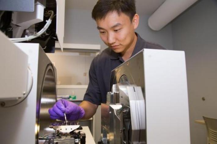
On The Scope – A Masterclass in Practical Scanning Electron Microscopy is a training program covering the fundamentals and advanced techniques of scanning electron microscopy (SEM) operation. Attendees will learn SEM techniques from world leading faculty and experts. They will work alongside experienced CEMAS staff hands-on the microscopes. Participants register for the 2 component class. The first component is a series of asynchronous lectures delivered online. For the second component participants register for the 2 day group lab session on May 4-6, 2027 (traditional lab track) or register for an individual flexible timing half day focused on registrant interests (individual track). Additional add-on SEM time working with CEMAS experts to dive into techniques and samples is available upon request.
Delivery Options
Hybrid: This program combines asynchronous online learning with an in-person laboratory component. Participants complete the online coursework and then attend either the Traditional Group Lab Track or the Flexible Individual Track.
Time to Completion
This program is projected to take approximately 45 hours to complete.
Course Completion Requirements
Successful completion of this course requires earning a score of at least 80% on required assessments and completing all required program components.
Technology Requirements
- Reliable internet connection
- Computer, laptop, or tablet capable of accessing online course materials
- Ability to stream video and interactive content
- Recommended browsers: Google Chrome or Firefox
What You'll Learn
- Describe the basic components of an SEM column.
- Explain the differences between SEMs and other electron/x-ray imaging techniques.
- Recognize the applications for which SEMs are most suitable.
- Understand the types of signals generated within SEM chambers.
- Relate the importance of proper preparation for different types of SEM samples.
- Define and describe all relevant imaging terminology (resolution, pixel size, field width, etc.).
- Relate the differences between information contained in images formed by various types of signals and detectors.
- Understand how different microscope and acquisition settings affect image quality.
- Demonstrate how to acquire different types of images.
- Explain how different material types require different imaging strategies.
- Understand the process of EDS data collection and analysis.
- Describe the advantages and disadvantages between spot, line, and map collection schemes, and explain when each type is most appropriate.
- Relate the importance of proper sample preparation for EDS analysis.
- Explain the factors limiting accuracy and resolution of EDS results, especially quantification.
- Demonstrate how to identify different elements present in a material.
- Explain the different types of information obtainable through EBSD.
- Relate the importance of proper sample preparation for EBSD analysis.
- Explain the origins of Kikuchi patterns and the process of indexing them.
- Describe the different types of resolution in the context of EBSD.
- Demonstrate the process of EBSD data acquisition and analysis.
- Describe immersion lenses and explain their effects.
- Define energy thresholding and demonstrate how to use it.
- Define stage biasing and demonstrate how to use it.
- Describe the benefits and limitations of variable pressure SEM operation.
- Explain STEM imaging in SEMs, including its benefits and limitations.
- Explain the TKD analysis process and its benefits and limitations.
- Describe cathodoluminescence and what information it provides.
What You'll Earn
- A certificate of completion from Ohio State University College of Engineering.
Program Component Details
Component #1 for ALL On The Scope Participants
Course content and lectures will be available through asynchronous online learning. A series of online lectures and demonstration sessions are presented by leading experts from The Ohio State University and industry partners and provide the foundation for the hands-on laboratory experience.
- Introduction to scanning electron microscopy (SEM)
- Electron sources probe formation
- Detectors in the SEM
- Sample Prep
- High resolution imaging
- Non-conductive sample imaging
- Energy dispersive X-Ray spectroscopy (EDS)
- Electron backscatter diffraction (EBSD)
- Cathodoluminescence
- In-situ/environmental SEM
- STEM in SEM
- Intro to FIB
- Semiconductor defect analysis
- Metallography/fractography
- Image analysis
- EDS data analysis
- EBSD data analysis
- Large area Imaging
Flexible Individual Track Component #2
4-Hour Instrument Session (Scheduled After Registration)
Participants schedule a one-on-one workshop with expert CEMAS staff for hands-on microscope training focused on participant interests, applications, and sample types. Imaging and demonstration can be performed using participant-provided samples.
Traditional Group Lab Track Component #2
May 4-6, 2027
The labs are delivered in person using the educational facilities and instrumentation available at CEMAS. Participants work directly with expert staff to develop practical microscopy skills through structured laboratory activities.
Schedule is tentative and subject to change.
| Time | Lab Day 1 | Lab Day 2 |
|---|---|---|
| 8:00 AM - 10:00 AM | Basic Imaging | Advanced Lab |
| 10:00 AM - 10:30 AM | Coffee Break | Coffee Break |
| 10:30 AM - 12:30 PM | Alignments | Advanced Lab |
| 12:30 PM - 1:30 PM | Lunch Break / Optional CEMAS Tour | Lunch Break |
| 1:30 PM - 3:30 PM | Advanced Modes OR EDS | Advanced Lab |
| 3:30 PM - 4:00 PM | Coffee Break | Coffee Break |
| 4:00 PM - 6:00 PM | Advanced Modes OR EDS | Advanced Lab |
- Basic imaging
- Instrument alignment
- Advanced imaging detectors
- EDS
- Electron backscatter diffraction
- Cathodoluminescence
- Large area imaging
- Metallographic analysis
- Semiconductor imaging
- Biological sample imaging
- In-situ/environmental SEM
- STEM in SEM
- Variable pressure SEM/non-conductive imaging
- Advanced EDS
- Ultra-high resolution imaging
Contact Us
For questions about the enrollment process, payment options, technology, or course records, please submit an inquiry and our Enrollment Support team will assist you within 24 hours during business days.
For questions regarding the program, registration options, laboratory tracks, or instructional content, please contact:
Daniel Veghte
Email: veghte.2@osu.edu
CEMAS Administration
Email: cemas@osu.edu
Website: https://cemas.osu.edu